1.4.1.4 Fail Safe Update Memory layout for MIPS based MCUs
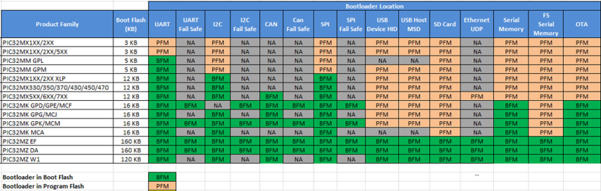
Bootloader placement for various PIC32M product families
The bootloader is placed in Boot Flash Memory (BFM) or Program Flash Memory (PFM) based on the size of the bootloader and available Boot flash memory on the device.
If the bootloader fits into the available BFM, it is placed in BFM. The user application can use the complete area of the program Flash memory.
If the bootloader does not fit into the available BFM, its reset handler is placed in BFM and rest of code is placed in PFM. The user application can use the remaining area of the program Flash memory.
The following table shows the available Boot Flash memory and the placement of different bootloaders by product family.
Note:
The Boot Flash and Program Flash memory end addresses may vary from device to device. Refer to respective Data sheets for details of Flash memory layout.
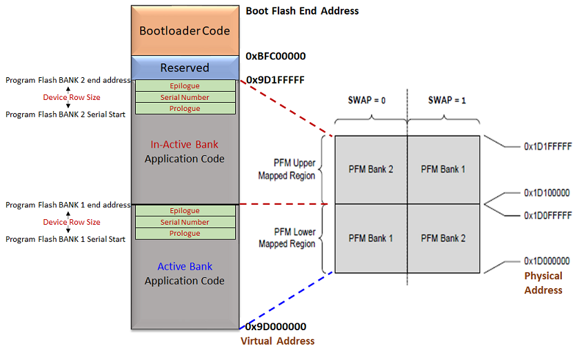
Fail Safe Update layout
Supported for the devices which have a Dual Bank flash memory
Bootloader code is placed at start of the Boot flash memory (0xBFC00000) as upon reset the device runs from start of boot flash memory.
Device always executes the application firmware from PFM bank mapped to lower memory region (0x1D00_0000 Physical address)
Start address of Active Bank is mapped to lower region 0x9D000000
Start address of Inactive Bank is from mid of the PFM which can vary from device to device. Refer to respective Data sheets for details of Flash memory layout.
Row size number of bytes are reserved at end of each bank for storing serial number. This serial number will be used by the bootloader code placed in BFM to map the appropriate PFM bank to lower memory region and run the application from there
Volatile register SWAP bit is used to map either of bank to lower memory region by bootloader
When Bootloader is running it will program the new image in the inactive bank and performs below operation and initiates a reset
Inactive Serial number = Active serial number + 1
At reset bootloader first maps Bank 1 to lower region and reads the serial numbers from both banks
If Bank 2 serial number is greater than Bank 1 serial number, it maps Bank 2 to lower region by setting the Swap bit and runs the new firmware. Now Bank 2 is Active bank
The application start address should always fall into lower mapped region (0x9D000000 to Mid of Flash). Size of the application in the linker script should also not exceed the Mid of flash.
The address passed to bootloader during programming should fall either in active bank or inactive bank based on update being done.