1.4.1.3 Fail Safe Update Memory layout for CORTEX-M based MCUs
Supported for the devices which have a Dual Bank flash memory
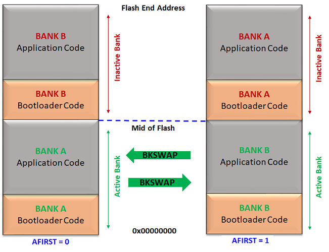
Internal Flash memory is split into two equal banks. Special NVM Fuse setting (AFIRST) is used to identify which bank is mapped to NVM main address space after reset.
Start address of Active Bank is always start of Internal Flash memory
Start address of Inactive Bank is from mid of the Internal flash memory which can vary from device to device. Refer to respective Data sheets for details of Flash memory layout.
Bootloader must be placed at start location of both banks
The application code can be placed anywhere after the bootloader end address till mid of flash. The application start address should be aligned to Erase Unit Size of the device
As the Bootloader code requires the application start address to be mentioned at compile time, it should match in both the application and bootloader
Bootloader running from Active bank will program the new image in inactive bank
Bootloader is responsible to perform a bank swap and reset to run the new firmware programmed in Inactive bank