
1.3.1.3.1 Abbreviations and Acronyms
| Abbreviation | Description |
|---|---|
| ADC |
Analog-to-Digital Converter consisting of a PGA, a second-order Δ/Σ modulator and followed by an integrated third-order sinc3 decimation filter. A digitized conversion of an analog voltage, VADCin, is created using the following equation: 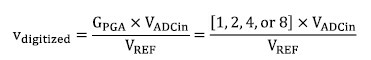 For best linearity, the product of ADC input voltage and the PGA gain must not exceed 0.5V, GPGA×VADCin≤0.5V, where GPGA for all voltage channels is fixed at 1. |
| AFE | Analog Front End |
| API | Application Programming Interface |
| Δ/Σ ADC | Delta-Sigma Analog-to-Digital Converter, an over-sampled converter with noise shaping |
| CT | Current Transformer sensor |
| DB | Demo Board |
| DNP | Do Not Populate |
| DSP | Digital Signal Processor |
| GPIO | General Purpose Input/Output |
| I_Ni | Imputed neutral current |
| I_Nm | Measured neutral current |
| I_Nmi | Difference between the measured and imputed neutral currents |
| Kh | Watt-hour meter constant for electro-mechanical meters, defines an amount of energy indicated by one (1) pulse generated by the meter and does not usually apply to solid-state meters |
| Kt | Watt-hour meter test constant for solid-state meters, defines an amount of energy indicated by one (1) optical pulse generated by the meter and does not usually apply to electro-mechanical meters |
| LCD | Liquid Crystal Display |
| MCU | Microcontroller Unit |
| MSB | Most Significant Bit, the left-most bit of a binary number |
| N | The number of samples in any one measurement interval. This number may vary for each measurement interval |
| NA | Not Available |
| OSR | Over Sample Rate |
| PGA | Programmable Gain Amplifier: The ADC channels associated with current measurement have an internal, selectable, programmable gain amplifier, which can provide an additional analog gain equal to GPGA. GPGA = [1, 2, 4 or 8] |
| SDK | Software Development Kit |
| SoC | System-on-Chip |
| TOU | Time of Use |
| VP, VP-N |
Voltage potential: VP is the voltage measured from node P to an explicit neutral reference voltage VP-M is the voltage measured from node P to node N, where a positive voltage is indicative of a voltage rise from node N to node P. All phase diagrams are drawn as if mathematical vectors starting at 0° (3 o’clock) and rotating counter-clockwise for positive phase increases, with 90° being at 12 o’clock, 180° at 9 o’clock and 270° at 6 o’clock. |