1.7.1.4 Live Update Memory layout for MIPS based MCUs
Supported for the devices which have a Dual Bank flash memory
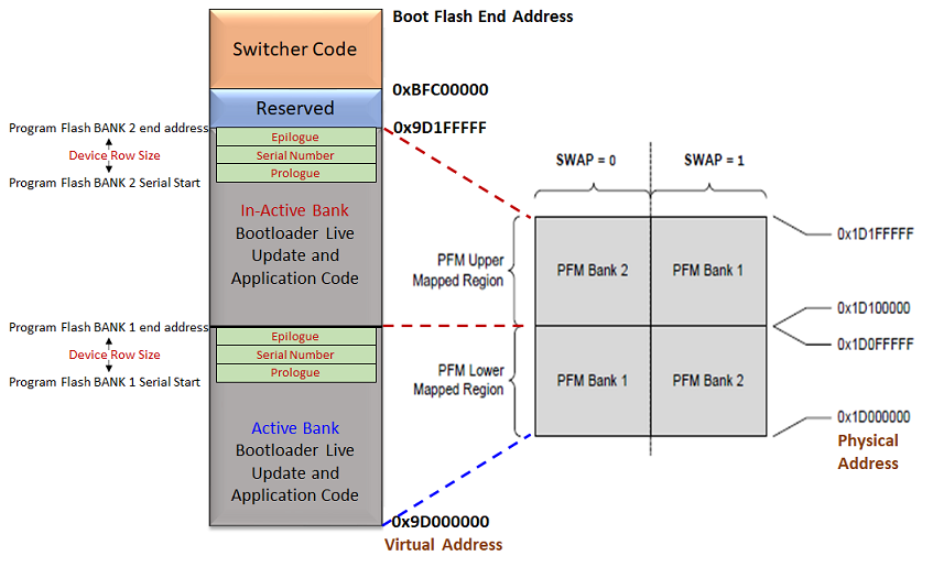
Switcher code is placed at start of the Boot flash memory (0xBFC00000) as upon reset the device runs from start of boot flash memory.
Note: The switcher code provided does not have any programming capabilities.It just performs bank swap operations
Device always executes the application firmware from PFM bank mapped to lower memory region (0x1D00_0000 Physical address)
Start address of Active Bank is mapped to lower region 0x9D000000
Start address of Inactive Bank is from mid of the PFM which can vary from device to device. Refer to respective Data sheets for details of Flash memory layout.
Row size number of bytes are reserved at end of each bank for storing serial number. This serial number will be used by the switcher code placed in BFM to map the appropriate PFM bank to lower memory region and run the application from there
Volatile register SWAP bit is used to map either of bank to lower memory region by switcher
The bootloader live update code responsible to program the inactive bank is part of the application it self. Which means the programming operation can happen while the application is running
Live Update Application = (Bootloader Code in Live Update mode + Application code)
The application code is responsible to send a request to bootloader live update code to perform a bank swap and reset to run the new firmware programmed in Inactive bank
Once this request is received the bootloader live update code performs below operation before initiating a reset to run new firmware
Inactive Serial number = Active serial number + 1
At reset switcher first maps Bank 1 to lower region and reads the serial numbers from both banks
If Bank 2 serial number is greater than Bank 1 serial number, it maps Bank 2 to lower region by setting the Swap bit and runs the new firmware. Now Bank 2 is Active bank
The live update start address should always fall into lower mapped region (0x9D000000 to Mid of Flash). Size of the application in the linker script should also not exceed the Mid of flash.