1.7.1.3 Live Update Memory layout for CORTEX-M based MCUs
Supported for the devices which have a Dual Bank flash memory
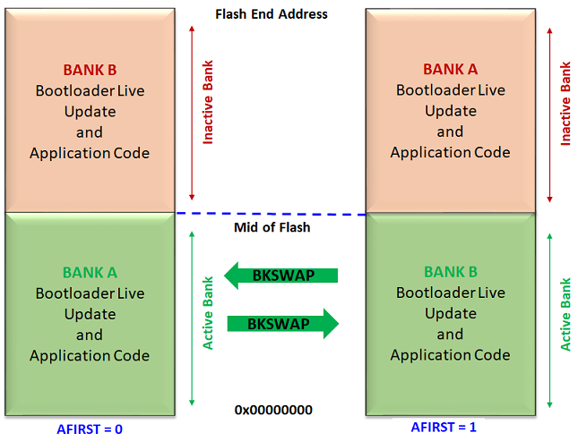
Internal Flash memory is split into two equal banks. Special NVM Fuse setting (AFIRST) is used to identify which bank is mapped to NVM main address space after reset.
Start address of Active Bank is always start of Internal Flash memory
Start address of Inactive Bank is from mid of the Internal flash memory which can vary from device to device. Refer to respective Data sheets for details of Flash memory layout.
The bootloader live update code responsible to program the inactive bank is part of the application it self. Which means the programming operation can happen while the application is running
Live Update Application = (Bootloader Code in Live Update mode + Application code)
Having the bootloader as part of application itself avoids the overhead of memory partitioning and saves flash memory.
The application code is responsible to send a request to bootloader live update code to perform a bank swap and reset to run the new firmware programmed in Inactive bank