
DRV_PLC_PHY_IDs
PLC_ID_HOST_DESCRIPTION_ID (0x0100)
Description: Name of MCU, in string format, where PL360 Host Controller is running.
Access: Read-only.
Value Range: 10 bytes.
Default Value: "SAME70" or "PIC32CX".
PLC_ID_HOST_MODEL_ID (0x010A)
Description: Model identification number of the PL360 Host Controller.
Access: Read-only.
Value Range: 2 bytes.
Default Value: 0x0002.
PLC_ID_HOST_PHY_ID (0x010C)
Description: Physical identification number of the PL360 Host Controller. It is composed of PLC_ID_HOST_VERSION_ID (0x0112) + PLC_ID_HOST_BAND_ID (0x0116).
Access: Read-only.
Value Range: 4 bytes.
Default Value: 0x36010104 (CENELEC-A), 0x36020104 (FCC) or 0x36040104 (CENELEC-B).
PLC_ID_HOST_PRODUCT_ID (0x0110)
Description: Product identification number of the PL360 Host Controller.
Access: Read-only.
Value Range: 2 bytes.
Default Value: 0x3601.
PLC_ID_HOST_VERSION_ID (0x0112)
Description: Version number of the PL360 Host Controller.
Access: Read-only.
Value Range: 4 bytes.
Default Value: 0x36010200.
PLC_ID_HOST_BAND_ID (0x0116)
Description: Workband identification number of the PL360 Host Controller.
Access: Read-only.
Value Range: 1 byte.
Default Value: 1: CENELEC A, 2: FCC, 4: CENELEC B.
PLC_ID_TIME_REF_ID (0x0200)
Description: Time reference in microseconds from the last reset of the PL360 device.
Access: Read-only.
Value Range: 4 bytes.
Default Value: Not applicable.
PLC_ID_PRODID (0x4000)
Description: Product Identifier of firmware embedded in PL360 device.
Access: Read-only.
Value Range: 8 bytes.
Default Value: "ATPL360B".
PLC_ID_MODEL (0x4001)
Description: Model Identifier of firmware embedded in PL360 device.
Access: Read-only.
Value Range: 2 bytes.
Default Value: 0x3601.
PLC_ID_VERSION_STR (0x4002)
Description: Version number of PL360 PHY embedded firmware in string format. The format is "AA.BB.CC.DD", where:
AA: Corresponds to device model ("36")
BB: Corresponds to G3 band
CC: Major version number
DD: Minor version number
Access: Read-only.
Value Range: 11 bytes.
Example Value: "36.01.05.04".
PLC_ID_VERSION_NUM (0x4003)
Description: Version number of PL360 PHY embedded firmware in hexadecimal format. The format is 0xAABBCCDD, where:
AA: Corresponds to device model (0x36)
BB: Corresponds to G3 band
CC: Major version number
DD: Minor version number
Access: Read-only.
Value Range: 4 bytes.
Example Value: 0x36010504.
PLC_ID_TONE_MASK (0x4004)
Description: Configure Tone Mask (Static Notching). For each carrier in the corresponding G3-PLC band, there is one byte indicating whether the carrier is used or masked . The minimum number of used carriers is 6. The following figures show the carrier frequencies in different bands and its encoding on the PIB:
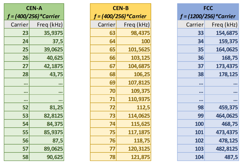
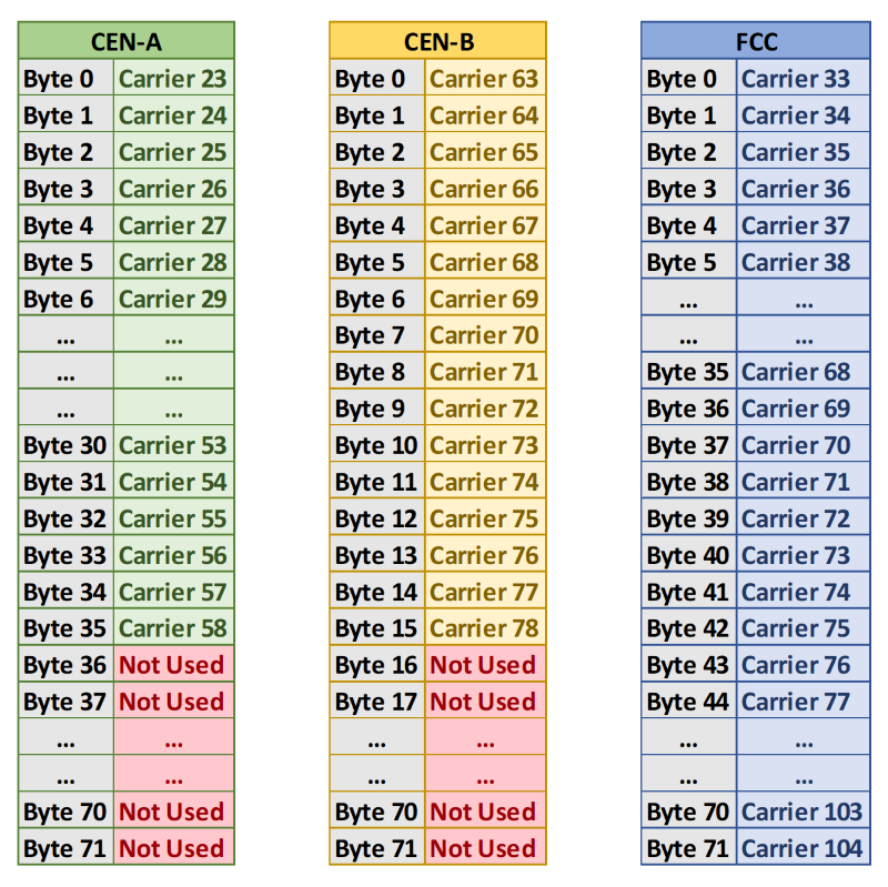
Access: Read-write.
Value Range: 36 bytes (CENELEC-A), 72 bytes (FCC) or 16 bytes (CENELEC-B).
Default Value: All 0s.
PLC_ID_TONE_MAP_RSP_DATA (0x4005)
Description: Tone Map response data is the best modulation and Tone Map combination to maximize baud rate and minimize frame error rate. It is calculated by the selection algorithm, based on the signal quality of the last received message. See PLC_ID_TONE_MAP_RSP_ENABLED_MODS (0x403E) to enable/disable the different modulations for the selection algorithm. The format is defined by the structure shown below:
typedef struct {
  // Modulation type
  DRV_PLC_PHY_MOD_TYPE modType;
  // Modulation scheme
  DRV_PLC_PHY_MOD_SCHEME modScheme;
  // Tone Map
  uint8_t toneMap[TONE_MAP_SIZE_MAX];
} DRV_PLC_PHY_TONE_MAP_RSP;
Access: Read-only.
Value Range: 5 bytes.
Default Value: BPSK Robust modulation type (0x04), differential modulation scheme (0x00) and full tone map (0x3F0000 in CENELEC-A; 0x0F0000 in CENELEC-B; 0xFFFFFF in FCC).
PLC_ID_TX_TOTAL (0x4006)
Description: Number of successfully transmitted PDUs.
Access: Read-write.
Value Range: 4 bytes.
Default Value: 0.
PLC_ID_TX_TOTAL_BYTES (0x4007)
Description: Number of bytes in successfully transmitted PDUs.
Access: Read-write.
Value Range: 4 bytes.
Default Value: 0.
PLC_ID_TX_TOTAL_ERRORS (0x4008)
Description: Number of unsuccessfully transmitted PDUs.
Access: Read-write.
Value Range: 4 bytes.
Default Value: 0.
PLC_ID_TX_BAD_BUSY_TX (0x4009)
Description: Number of times when the PL360 device received new data to transmit (send_data) and there is already data in the TX chain.
Access: Read-write.
Value Range: 4 bytes.
Default Value: 0.
PLC_ID_TX_BAD_BUSY_CHANNEL (0x400A)
Description: Number of times when the PL360 device received new data to transmit (send_data) and the PLC channel is busy.
Access: Read-write.
Value Range: 4 bytes.
Default Value: 0.
PLC_ID_TX_BAD_LEN (0x400B)
Description: Number of times when the PL360 device received new data to transmit (send_data) and the specified length in transmission parameters is invalid.
Access: Read-write.
Value Range: 4 bytes.
Default Value: 0.
PLC_ID_TX_BAD_FORMAT (0x400C)
Description: Number of times when the PL360 device received new data to transmit (send_data) and the transmission parameters are not valid.
Access: Read-write.
Value Range: 4 bytes.
Default Value: 0.
PLC_ID_TX_TIMEOUT (0x400D)
Description: Number of times when the PL360 device received new data to transmit (send_data) and it cannot transmit data in the specified time provided by the transmission parameters.
Access: Read-write.
Value Range: 4 bytes.
Default Value: 0.
PLC_ID_RX_TOTAL (0x400E)
Description: Number of successfully received PDUs.
Access: Read-write.
Value Range: 4 bytes.
Default Value: 0.
PLC_ID_RX_TOTAL_BYTES (0x400F)
Description: Number of bytes in successfully received PDUs.
Access: Read-write.
Value Range: 4 bytes.
Default Value: 0.
PLC_ID_RX_RS_ERRORS (0x4010)
Description: Number of corrected errors by RS block in received PDUs.
Access: Read-write.
Value Range: 4 bytes.
Default Value: 0.
PLC_ID_RX_EXCEPTIONS (0x4011)
Description: Number of time-out errors in received PDUs.
Access: Read-write.
Value Range: 4 bytes.
Default Value: 0.
PLC_ID_RX_BAD_LEN (0x4012)
Description: Number of errors in FCH length in received PDUs.
Access: Read-write.
Value Range: 4 bytes.
Default Value: 0.
PLC_ID_RX_BAD_CRC_FCH (0x4013)
Description: Number of errors in FCH CRC in received PDUs.
Access: Read-write.
Value Range: 4 bytes.
Default Value: 0.
PLC_ID_RX_FALSE_POSITIVE (0x4014)
Description: Number of errors in PDU synchronization phase.
Access: Read-write.
Value Range: 4 bytes.
Default Value: 0.
PLC_ID_RX_BAD_FORMAT (0x4015)
Description: Number of errors in modulation type field included in FCH of received PDUs.
Access: Read-write.
Value Range: 4 bytes.
Default Value: 0.
PLC_ID_ENABLE_AUTO_NOISE_CAPTURE (0x4016)
Description: Flag to indicate if automatic noise analyzer is enabled in the reception chain. If Auto-mode is enabled, notch filter parameters (PLC_ID_RRC_NOTCH_ACTIVE (0x4019), PLC_ID_RRC_NOTCH_INDEX (0x401A)) cannot be modified by the user. See PLC_ID_TIME_BETWEEN_NOISE_CAPTURES (0x4017), PLC_ID_RRC_NOTCH_THR_ON (0x4034), PLC_ID_RRC_NOTCH_THR_OFF (0x4035) to configure parameters related to the Auto-mode.
Access: Read-write.
Value Range: 1 byte .
Default Value: 1.
PLC_ID_TIME_BETWEEN_NOISE_CAPTURES (0x4017)
Description: Time in milliseconds between noise captures.
Access: Read-write.
Value Range: 4 bytes.
Default Value: 1000 (1 second).
CAUTION: It is recommended that the default value of this parameter be kept. If reduced, the power consumption could increase. The default value is optimum for power consumption and performance of noise detection.
PLC_ID_DELAY_NOISE_CAPTURE_AFTER_RX (0x4018)
Description: Time in microseconds to start a new noise capture after PDU reception/transmission.
Access: Read-write.
Value Range: 4 bytes .
Default Value: 3000 (3 milliseconds).
PLC_ID_RRC_NOTCH_ACTIVE (0x4019)
Description: Number of notched frequencies with RRC notch filter. For CENELEC-A and FCC bands, up to 5 notched frequencies are allowed. For CENELEC-B band, only one notched frequency is allowed.
Access: Depends on noise analyzer mode PLC_ID_ENABLE_AUTO_NOISE_CAPTURE (0x4016) value:
Auto-mode (1): Read-only
Manual-mode (0): Read-write
Value Range: 1 byte .
Default Value: 0 (No notched frequencies).
PLC_ID_RRC_NOTCH_INDEX (0x401A)
Description: Array of RRC notch filter index values. There is one index for each notched frequency. The format of each index is uQ7.8 (2 bytes, where MSB must be 0). The 7 integer bits indicate the carrier index for which the notch filter is applied. The 8 decimal bits can apply the notch filter to a frequency that is between two consecutive carriers. To convert the notch index to frequency (in Hz), the following formula is applied:
F = INDEX * Fs / 65536 , where Fs is the sampling rate in Hz:
CENELEC-A, CENELEC-B bands: Fs = 400000 Hz
FCC band: Fs = 1200000 Hz
For example:
CENELEC-A, INDEX = 8192 (0x2000): F = 8192 * 400000 / 65536 = 50000 Hz
FCC, INDEX = 20544 (0x5040): F = 20544 * 1200000 / 65536 = 376172 Hz
Access: Depends on noise analyzer mode PLC_ID_ENABLE_AUTO_NOISE_CAPTURE (0x4016) value:
1 (Auto-mode): Read-only
0 (Manual-mode): Read-write
Value Range: 10 bytes (CENELEC-A, FCC bands) or 2 bytes (CENELEC-B band). Each group of 2 bytes corresponds to one notched frequency (Integer part: 0 - 127, Decimal part: 0-255). Number of valid values depends on PLC_ID_RRC_NOTCH_ACTIVE (0x4019).
Default Value: 0.
PLC_ID_NOISE_PEAK_POWER (0x401B)
Description: Estimation of noise level, in dBµV, for the carrier with highest noise power. It is actually the maximum value of the PIB described in PLC_ID_NOISE_PER_CARRIER (0x403A). The value is updated only if noise analyzer Auto-mode is enabled (PLC_ID_ENABLE_AUTO_NOISE_CAPTURE (0x4016)) or if noise capture is triggered manually (PLC_ID_RRC_NOTCH_AUTODETECT (0x4024)).
Access: Read-only.
Value Range: 2 bytes.
Default Value: 0.
PLC_ID_CRC_TX_RX_CAPABILITY (0x401C)
Description: CRC computation capability. If it is enabled, 16-bit CRC is computed in transmitted and received PDUs. The CRC format is the same that uses the G3-PLC stack, which is described in the IEEE 802.15.4 standard. In transmission, when it is enabled, padding and CRC are added to the data automatically. In order to ensure that all OFDM symbols are filled with data, a zero-padding is inserted after data payload (if it is needed). The padding guarantees that the last 16 bits in reception correspond to the 16-bit CRC. The 16-bit CRC is added after the padding. In reception, when it is enabled, CRC is computed over the received PDU and it is compared to the last 16 bits of the data (corresponding to the CRC of the message) to check the integrity of the message. These two bytes are not included in the data buffer containing the received frame reported in DRV_PLC_PHY_RECEPTION_OBJ. The field crcOk in DRV_PLC_PHY_RECEPTION_OBJ shows whether the CRC is correct or not. Microchip G3-PLC stack implementation does not use this functionality, since CRC is computed in MAC layer instead of PHY layer. The aim of this PIB is to make it easier for customers to build applications over PHY layer.
Access: Read-write.
Value Range: 1 byte .
Default Value: 0.
PLC_ID_RX_BAD_CRC_PAY (0x401D)
Description: Number of errors in payload CRC in received PDUs. It is only updated if CRC capability is enabled (see PLC_ID_CRC_TX_RX_CAPABILITY (0x401C)).
Access: Read-write.
Value Range: 4 bytes.
Default Value: 0.
PLC_ID_CFG_AUTODETECT_IMPEDANCE (0x401E)
Description: Auto-Detect Impedance Mode. Transmission Automatic Gain Control (Tx AGC) and Automatic Transmission Mode Control (ATMC) can be enabled/disabled. There are 3 available modes:
OFF : Tx AGC disabled. ATMC disabled.
ON : Tx AGC enabled. ATMC enabled.
AGC : Tx AGC enabled. ATMC disabled.
Access: Read-write.
Value Range: 1 byte .
Default Value: 1.
PLC_ID_CFG_IMPEDANCE (0x401F)
Description: Transmission Mode (HIGH, LOW, VERY_LOW). It is automatically updated if ATMC is enabled (see PLC_ID_CFG_AUTODETECT_IMPEDANCE (0x401E)).
Access: Read-write.
Value Range: 1 byte .
Default Value: 0.
PLC_ID_ZC_PERIOD (0x4020)
Description: Last estimation of the mains Zero-Crossing period, in microseconds.
Access: Read-only.
Value Range: 4 bytes.
Default Value: 0.
PLC_ID_FCH_SYMBOLS (0x4021)
Description: Number of symbols in Frame Control Header. Depends on the G3 band in use and Tone Mask (see PLC_ID_TONE_MASK (0x4004)).
Access: Read-only.
Value Range: 1 byte .
Default Value: 13 (CENELEC-A), 12 (FCC), 30 (CENELEC-B).
PLC_ID_PAY_SYMBOLS_TX (0x4022)
Description: Number of payload symbols in the last requested transmission.
Access: Read-only.
Value Range: 2 bytes .
Default Value: 0.
PLC_ID_PAY_SYMBOLS_RX (0x4023)
Description: Number of payload symbols in last received message.
Access: Read-only.
Value Range: 2 bytes .
Default Value: 0.
PLC_ID_RRC_NOTCH_AUTODETECT (0x4024)
Description: Trigger to start noise analysis. If noise analyzer Manual-mode is enabled (see PLC_ID_ENABLE_AUTO_NOISE_CAPTURE (0x4016)), noise capture can be triggered through this PIB by writing 1. Writing 0 has no effect. If noise analyzer Auto-mode is enabled, writing any value has no effect.
Access: Write-only.
Value Range: 1 byte.
Default Value: 0.
PLC_ID_MAX_RMS_TABLE_HI (0x4025)
Description: Target value of RMS_CALC in HIGH Tx Mode (see PLC_ID_CFG_IMPEDANCE (0x401F)). RMS_CALC will tend to this value by automatically adjusting the gain after every transmission (see PLC_ID_CURRENT_GAIN (0x4036)). These parameters are only used if Tx AGC is enabled (see PLC_ID_CFG_AUTODETECT_IMPEDANCE (0x401E)).
Access: Read-write.
Value Range: 32 bytes.
| Byte 0-3 | Byte 4-7 | Byte 8-11 | Byte 12-15 | Byte 16-19 | Byte 20-24 | Byte 25-27 | Byte 28-31 |
|---|---|---|---|---|---|---|---|
| RMS_HI_0 | RMS_HI_1 | RMS_HI_2 | RMS_HI_3 | RMS_HI_4 | RMS_HI_5 | RMS_HI_6 | RMS_HI_7 |
where RMS_HI_x: Target value of RMS_CALC in mode of transmission HIGH for the attenuation level x (attenuation levels in 3dB steps)
Default Value:
| G3 BAND | RMS_HI_0 | RMS_HI_1 | RMS_HI_2 | RMS_HI_3 | RMS_HI_4 | RMS_HI_5 | RMS_HI_6 | RMS_HI_7 |
|---|---|---|---|---|---|---|---|---|
| CEN-A | 1991 | 1381 | 976 | 695 | 495 | 351 | 250 | 179 |
| FCC | 1355 | 960 | 681 | 485 | 345 | 246 | 177 | 129 |
| CEN-B | 1133 | 793 | 559 | 396 | 280 | 199 | 143 | 108 |
PLC_ID_MAX_RMS_TABLE_VLO (0x4026)
Description: Target value of RMS_CALC in VERY_LOW Tx Mode (see PLC_ID_CFG_IMPEDANCE (0x401F)). RMS_CALC will tend to this value by automatically adjusting the gain after every transmission (see PLC_ID_CURRENT_GAIN (0x4036)). These parameters are only used if Tx AGC is enabled (see PLC_ID_CFG_AUTODETECT_IMPEDANCE (0x401E)).
Access: Read-write.
Value Range: 32 bytes.
| Byte 0-3 | Byte 4-7 | Byte 8-11 | Byte 12-15 | Byte 16-19 | Byte 20-24 | Byte 25-27 | Byte 28-31 |
|---|---|---|---|---|---|---|---|
| RMS_VLO_0 | RMS_VLO_1 | RMS_VLO_2 | RMS_VLO_3 | RMS_VLO_4 | RMS_VLO_5 | RMS_VLO_6 | RMS_VLO_7 |
where: RMS_HI_x: Target value of RMS_CALC in mode of transmission VERY_LOW for the attenuation level x (attenuation levels in 3dB steps)
Default Value:
| G3 BAND | RMS_VLO_0 | RMS_VLO_1 | RMS_VLO_2 | RMS_VLO_3 | RMS_VLO_4 | RMS_VLO_5 | RMS_VLO_6 | RMS_VLO_7 |
|---|---|---|---|---|---|---|---|---|
| CEN-A | 6356 | 4706 | 3317 | 2308 | 1602 | 1112 | 778 | 546 |
| FCC | 5656 | 4174 | 2877 | 1987 | 1413 | 1020 | 736 | 532 |
| CEN-B | 2871 | 2120 | 1498 | 1054 | 740 | 519 | 366 | 259 |
PLC_ID_THRESHOLDS_TABLE_HI (0x4027)
Description: Table of thresholds to automatically update Tx Mode (see PLC_ID_CFG_IMPEDANCE (0x401F)) from HIGH mode. These parameters are only used if ATMC is enabled (see PLC_ID_CFG_AUTODETECT_IMPEDANCE (0x401E)). Corrected RMS_CALC (see PLC_ID_CORRECTED_RMS_CALC (0x4033)) is compared with these thresholds after every transmission to select Tx Mode for next transmission. The decision is taken following the steps shown below:
If corrected RMS_CALC is below TH_HI_VLO_x, Tx Mode will be updated to VERY_LOW mode
Else if corrected RMS_CALC is below TH_HI_LO_x, Tx Mode will be updated to LOW mode
Else Tx Mode will remain in HIGH mode
where:
TH_HI_VLO_x: Threshold to change from HIGH to VERY_LOW mode for Tx attenuation level x (3 dB steps)
TH_HI_LO_x: Threshold to change from HIGH to LOW mode for Tx attenuation level x (3 dB steps)
Access: Read-write.
Value Range: 64 bytes.
| Byte 0-3 | Byte 4-7 | Byte 8-11 | Byte 12-15 | Byte 16-19 | Byte 20-24 | Byte 25-27 | Byte 28-31 |
|---|---|---|---|---|---|---|---|
| TH_HI_LO_0 | TH_HI_LO_1 | TH_HI_LO_2 | TH_HI_LO_3 | TH_HI_LO_4 | TH_HI_LO_5 | TH_HI_LO_6 | TH_HI_LO_7 |
| Byte 32-35 | Byte 36-39 | Byte 40-43 | Byte 44-47 | Byte 48-51 | Byte 52-55 | Byte 56-59 | Byte 60-63 |
|---|---|---|---|---|---|---|---|
| TH_HI_VLO_0 | TH_HI_VLO_1 | TH_HI_VLO_2 | TH_HI_VLO_3 | TH_HI_VLO_4 | TH_HI_VLO_5 | TH_HI_VLO_6 | TH_HI_VLO_7 |
Default Value:
| G3 BAND | TH_HI_LO_0 | TH_HI_LO_1 | TH_HI_LO_2 | TH_HI_LO_3 | TH_HI_LO_4 | TH_HI_LO_5 | TH_HI_LO_6 | TH_HI_LO_7 |
|---|---|---|---|---|---|---|---|---|
| CEN-A | 0 | 0 | 0 | 0 | 0 | 0 | 0 | 0 |
| FCC | 0 | 0 | 0 | 0 | 0 | 0 | 0 | 0 |
| CEN-B | 0 | 0 | 0 | 0 | 0 | 0 | 0 | 0 |
| G3 BAND | TH_HI_VLO_0 | TH_HI_VLO_1 | TH_HI_VLO_2 | TH_HI_VLO_3 | TH_HI_VLO_4 | TH_HI_VLO_5 | TH_HI_VLO_6 | TH_HI_VLO_7 |
|---|---|---|---|---|---|---|---|---|
| CEN-A | 1685 | 1173 | 828 | 589 | 419 | 298 | 212 | 151 |
| FCC | 1147 | 811 | 576 | 409 | 291 | 208 | 150 | 109 |
| CEN-B | 950 | 667 | 471 | 334 | 238 | 169 | 122 | 90 |
PLC_ID_THRESHOLDS_TABLE_LO (0x4028)
Description: Table of thresholds to automatically update Tx Mode (see PLC_ID_CFG_IMPEDANCE (0x401F)) from LOW mode. These parameters are only used if ATMC is enabled (see PLC_ID_CFG_AUTODETECT_IMPEDANCE (0x401E)). Corrected RMS_CALC (see PLC_ID_CORRECTED_RMS_CALC (0x4033)) is compared with these thresholds after every transmission to select Tx Mode for next transmission. The decision is taken following the steps shown below:
If corrected RMS_CALC is below TH_LO_VLO_x, Tx Mode will be updated to VERY_LOW mode
Else if corrected RMS_CALC is above TH_LO_HI_x, Tx Mode will be updated to HIGH mode
Else Tx Mode will remain in LOW mode
where:
TH_LO_VLO_x: Threshold to change from LOW to VERY_LOW mode for Tx attenuation level x (3 dB steps)
TH_LO_HI_x: Threshold to change from LOW to HIGH mode for Tx attenuation level x (3 dB steps)
Access: Read-write.
Value Range: 64 bytes.
| Byte 0-3 | Byte 4-7 | Byte 8-11 | Byte 12-15 | Byte 16-19 | Byte 20-24 | Byte 25-27 | Byte 28-31 |
|---|---|---|---|---|---|---|---|
| TH_LO_HI_0 | TH_LO_HI_1 | TH_LO_HI_2 | TH_LO_HI_3 | TH_LO_HI_4 | TH_LO_HI_5 | TH_LO_HI_6 | TH_LO_HI_7 |
| Byte 32-35 | Byte 36-39 | Byte 40-43 | Byte 44-47 | Byte 48-51 | Byte 52-55 | Byte 56-59 | Byte 60-63 |
|---|---|---|---|---|---|---|---|
| TH_LO_VLO_0 | TH_LO_VLO_1 | TH_LO_VLO_2 | TH_LO_VLO_3 | TH_LO_VLO_4 | TH_LO_VLO_5 | TH_LO_VLO_6 | TH_LO_VLO_7 |
Default Value:
| G3 BAND | TH_LO_HI_0 | TH_LO_HI_1 | TH_LO_HI_2 | TH_LO_HI_3 | TH_LO_HI_4 | TH_LO_HI_5 | TH_LO_HI_6 | TH_LO_HI_7 |
|---|---|---|---|---|---|---|---|---|
| CEN-A | 0 | 0 | 0 | 0 | 0 | 0 | 0 | 0 |
| FCC | 0 | 0 | 0 | 0 | 0 | 0 | 0 | 0 |
| CEN-B | 0 | 0 | 0 | 0 | 0 | 0 | 0 | 0 |
| G3 BAND | TH_LO_VLO_0 | TH_LO_VLO_1 | TH_LO_VLO_2 | TH_LO_VLO_3 | TH_LO_VLO_4 | TH_LO_VLO_5 | TH_LO_VLO_6 | TH_LO_VLO_7 |
|---|---|---|---|---|---|---|---|---|
| CEN-A | 0 | 0 | 0 | 0 | 0 | 0 | 0 | 0 |
| FCC | 0 | 0 | 0 | 0 | 0 | 0 | 0 | 0 |
| CEN-B | 0 | 0 | 0 | 0 | 0 | 0 | 0 | 0 |
PLC_ID_THRESHOLDS_TABLE_VLO (0x4029)
Description: Table of thresholds to automatically update Tx Mode (see PLC_ID_CFG_IMPEDANCE (0x401F)) from VERY_LOW mode. These parameters are only used if ATMC is enabled (see PLC_ID_CFG_AUTODETECT_IMPEDANCE (0x401E)). Corrected RMS_CALC (see PLC_ID_CORRECTED_RMS_CALC (0x4033)) is compared with these thresholds after every transmission to select Tx Mode for next transmission. The decision is taken following the steps shown below:
If corrected RMS_CALC is below TH_VLO_VLO_x, Tx Mode will remain in VERY_LOW mode
Else if corrected RMS_CALC is above TH_VLO_HI_x, Tx Mode will be updated to HIGH mode
Else Tx Mode will be updated to LOW mode
where:
TH_VLO_VLO_x: Threshold to remain Tx mode in VERY_LOW mode for Tx attenuation level x (3 dB steps)
TH_VLO_HI_x: Threshold to change from VERY_LOW to HIGH mode for Tx attenuation level x (3 dB steps)
Access: Read-write.
Value Range: 64 bytes.
| Byte 0-3 | Byte 4-7 | Byte 8-11 | Byte 12-15 | Byte 16-19 | Byte 20-24 | Byte 25-27 | Byte 28-31 |
|---|---|---|---|---|---|---|---|
| TH_VLO_HI_0 | TH_VLO_HI_1 | TH_VLO_HI_2 | TH_VLO_HI_3 | TH_VLO_HI_4 | TH_VLO_HI_5 | TH_VLO_HI_6 | TH_VLO_HI_7 |
| Byte 32-35 | Byte 36-39 | Byte 40-43 | Byte 44-47 | Byte 48-51 | Byte 52-55 | Byte 56-59 | Byte 60-63 |
|---|---|---|---|---|---|---|---|
| TH_VLO_VLO_0 | TH_VLO_VLO_1 | TH_VLO_VLO_2 | TH_VLO_VLO_3 | TH_VLO_VLO_4 | TH_VLO_VLO_5 | TH_VLO_VLO_6 | TH_VLO_VLO_7 |
Default Value:
| G3 BAND | TH_VLO_HI_0 | TH_VLO_HI_1 | TH_VLO_HI_2 | TH_VLO_HI_3 | TH_VLO_HI_4 | TH_VLO_HI_5 | TH_VLO_HI_6 | TH_VLO_HI_7 |
|---|---|---|---|---|---|---|---|---|
| CEN-A | 0 | 0 | 0 | 0 | 0 | 0 | 0 | 0 |
| FCC | 0 | 0 | 0 | 0 | 0 | 0 | 0 | 0 |
| CEN-B | 0 | 0 | 0 | 0 | 0 | 0 | 0 | 0 |
| G3 BAND | TH_VLO_VLO_0 | TH_VLO_VLO_1 | TH_VLO_VLO_2 | TH_VLO_VLO_3 | TH_VLO_VLO_4 | TH_VLO_VLO_5 | TH_VLO_VLO_6 | TH_VLO_VLO_7 |
|---|---|---|---|---|---|---|---|---|
| CEN-A | 8988 | 6370 | 4466 | 3119 | 2171 | 1512 | 1061 | 752 |
| FCC | 8153 | 5718 | 4007 | 2871 | 2080 | 1506 | 1083 | 778 |
| CEN-B | 3878 | 2749 | 1935 | 1362 | 965 | 686 | 493 | 353 |
PLC_ID_PREDIST_COEF_TABLE_HI (0x402A)
Description: Equalization Coefficients table in HIGH Tx mode. There is one coefficient for each carrier in the used band. The format of each coefficient is uQ0.16 (2 bytes). PL360 firmware compensates the total gain internally, so modifying the digital gain (see PLC_ID_GAIN_TABLE_HI (0x402D)) is not needed when equalization is modified.
Access: Read-write.
Value Range: 72 bytes (CENELEC-A), 32 bytes (CENELEC-B) or 144 bytes (FCC).
Default Value:
CENELEC-A:
{0x670A, 0x660F, 0x676A, 0x6A6B, 0x6F3F, 0x7440, 0x74ED, 0x7792, 0x762D, 0x7530, 0x7938, 0x7C0A, 0x7C2A, 0x7B0E, 0x7AF2, 0x784B, 0x7899, 0x76F9, 0x76D6, 0x769F, 0x775D, 0x70C0, 0x6EB9, 0x6F18, 0x6F1E, 0x6FA2, 0x6862, 0x67C9, 0x68F9, 0x68A5, 0x6CA3, 0x7153, 0x7533, 0x750B, 0x7B59, 0x7FFF}
FCC:
{0x7FFF, 0x7FFF, 0x7FFF, 0x7FFF, 0x7FFF, 0x7FFF, 0x7FFF, 0x7FFF, 0x7FFF, 0x7FFF, 0x7FFF, 0x7FFF, 0x7FFF, 0x7FFF, 0x7FFF, 0x7FFF, 0x7FFF, 0x7FFF, 0x7FFF, 0x7FFF, 0x7FFF, 0x7FFF, 0x7FFF, 0x7FFF, 0x7FFF, 0x7FFF, 0x7FFF, 0x7FFF, 0x7FFF, 0x7FFF, 0x7FFF, 0x7FFF, 0x7FFF, 0x7FFF, 0x7FFF, 0x7FFF, 0x7FFF, 0x7FFF, 0x7FFF, 0x7FFF, 0x7FFF, 0x7FFF, 0x7FFF, 0x7FFF, 0x7FFF, 0x7FFF, 0x7FFF, 0x7FFF, 0x7FFF, 0x7FFF, 0x7FFF, 0x7FFF, 0x7FFF, 0x7FFF, 0x7FFF, 0x7FFF, 0x7FFF, 0x7FFF, 0x7FFF, 0x7FFF, 0x7FFF, 0x7FFF, 0x7FFF, 0x7FFF, 0x7FFF, 0x7FFF, 0x7FFF, 0x7FFF, 0x7FFF, 0x7FFF, 0x7FFF, 0x7FFF}
CENELEC-B:
{0x7FFF, 0x7FFF, 0x7FFF, 0x7FFF, 0x7FFF, 0x7FFF, 0x7FFF, 0x7FFF, 0x7FFF, 0x7FFF, 0x7FFF, 0x7FFF, 0x7FFF, 0x7FFF, 0x7FFF, 0x7FFF}
PLC_ID_PREDIST_COEF_TABLE_LO (0x402B)
Description: Equalization Coefficients table in LOW Tx mode. There is one coefficient for each carrier in the used band. The format of each coefficient is uQ0.16 (2 bytes). PL360 firmware compensates the total gain internally, so modifying the gain it is not needed (see PLC_ID_GAIN_TABLE_LO (0x402E)) when equalization is modified.
Access: Read-write.
Value Range: 72 bytes (CENELEC-A), 32 bytes (CENELEC-B) or 144 bytes (FCC).
Default Value:
CENELEC-A:
{0x7FFF, 0x7DB1, 0x7CE6, 0x7B36, 0x772F, 0x7472, 0x70AA, 0x6BC2, 0x682D, 0x6618, 0x6384, 0x6210, 0x61D7, 0x6244, 0x6269, 0x63A8, 0x6528, 0x65CC, 0x67F6, 0x693B, 0x6B13, 0x6C29, 0x6D43, 0x6E26, 0x6D70, 0x6C94, 0x6BB5, 0x6AC9, 0x6A5F, 0x6B65, 0x6B8C, 0x6A62, 0x6CEC, 0x6D5A, 0x6F9D, 0x6FD3}
FCC:
{0x7FFF, 0x7FFF, 0x7FFF, 0x7FFF, 0x7FFF, 0x7FFF, 0x7FFF, 0x7FFF, 0x7FFF, 0x7FFF, 0x7FFF, 0x7FFF, 0x7FFF, 0x7FFF, 0x7FFF, 0x7FFF, 0x7FFF, 0x7FFF, 0x7FFF, 0x7FFF, 0x7FFF, 0x7FFF, 0x7FFF, 0x7FFF, 0x7FFF, 0x7FFF, 0x7FFF, 0x7FFF, 0x7FFF, 0x7FFF, 0x7FFF, 0x7FFF, 0x7FFF, 0x7FFF, 0x7FFF, 0x7FFF, 0x7FFF, 0x7FFF, 0x7FFF, 0x7FFF, 0x7FFF, 0x7FFF, 0x7FFF, 0x7FFF, 0x7FFF, 0x7FFF, 0x7FFF, 0x7FFF, 0x7FFF, 0x7FFF, 0x7FFF, 0x7FFF, 0x7FFF, 0x7FFF, 0x7FFF, 0x7FFF, 0x7FFF, 0x7FFF, 0x7FFF, 0x7FFF, 0x7FFF, 0x7FFF, 0x7FFF, 0x7FFF, 0x7FFF, 0x7FFF, 0x7FFF, 0x7FFF, 0x7FFF, 0x7FFF, 0x7FFF, 0x7FFF}
CENELEC-B:
{0x7FFF, 0x7FFF, 0x7FFF, 0x7FFF, 0x7FFF, 0x7FFF, 0x7FFF, 0x7FFF, 0x7FFF, 0x7FFF, 0x7FFF, 0x7FFF, 0x7FFF, 0x7FFF, 0x7FFF, 0x7FFF}
PLC_ID_PREDIST_COEF_TABLE_VLO (0x402C)
Description: Equalization Coefficients table in VERY_LOW Tx mode. There is one coefficient for each carrier in the used band. The format of each coefficient is uQ0.16 (2 bytes). PL360 firmware compensates the total gain internally, so modifying the gain is not needed (see PLC_ID_GAIN_TABLE_VLO (0x402F)) when equalization is modified.
Access: Read-write.
Value Range: 72 bytes (CENELEC-A), 32 bytes (CENELEC-B) or 144 bytes (FCC).
Default Value:
CENELEC-A:
{0x7FFF, 0x7DB1, 0x7CE6, 0x7B36, 0x772F, 0x7472, 0x70AA, 0x6BC2, 0x682D, 0x6618, 0x6384, 0x6210, 0x61D7, 0x6244, 0x6269, 0x63A8, 0x6528, 0x65CC, 0x67F6, 0x693B, 0x6B13, 0x6C29, 0x6D43, 0x6E26, 0x6D70, 0x6C94, 0x6BB5, 0x6AC9, 0x6A5F, 0x6B65, 0x6B8C, 0x6A62, 0x6CEC, 0x6D5A, 0x6F9D, 0x6FD3}
FCC:
{0x7FFF, 0x7FFF, 0x7FFF, 0x7FFF, 0x7FFF, 0x7FFF, 0x7FFF, 0x7FFF, 0x7FFF, 0x7FFF, 0x7FFF, 0x7FFF, 0x7FFF, 0x7FFF, 0x7FFF, 0x7FFF, 0x7FFF, 0x7FFF, 0x7FFF, 0x7FFF, 0x7FFF, 0x7FFF, 0x7FFF, 0x7FFF, 0x7FFF, 0x7FFF, 0x7FFF, 0x7FFF, 0x7FFF, 0x7FFF, 0x7FFF, 0x7FFF, 0x7FFF, 0x7FFF, 0x7FFF, 0x7FFF, 0x7FFF, 0x7FFF, 0x7FFF, 0x7FFF, 0x7FFF, 0x7FFF, 0x7FFF, 0x7FFF, 0x7FFF, 0x7FFF, 0x7FFF, 0x7FFF, 0x7FFF, 0x7FFF, 0x7FFF, 0x7FFF, 0x7FFF, 0x7FFF, 0x7FFF, 0x7FFF, 0x7FFF, 0x7FFF, 0x7FFF, 0x7FFF, 0x7FFF, 0x7FFF, 0x7FFF, 0x7FFF, 0x7FFF, 0x7FFF, 0x7FFF, 0x7FFF, 0x7FFF, 0x7FFF, 0x7FFF, 0x7FFF}
CENELEC-B:
{0x7FFF, 0x7FFF, 0x7FFF, 0x7FFF, 0x7FFF, 0x7FFF, 0x7FFF, 0x7FFF, 0x7FFF, 0x7FFF, 0x7FFF, 0x7FFF, 0x7FFF, 0x7FFF, 0x7FFF, 0x7FFF}
PLC_ID_GAIN_TABLE_HI (0x402D)
Description: Table of gain values for HIGH Tx Mode.
Access: Read-write.
Value Range: 6 bytes
| Byte 0-1 | Byte 2-3 | Byte 4-5 |
|---|---|---|
| GAIN_HI_INI | GAIN_HI_MIN | GAIN_HI_MAX |
where:
GAIN_HI_INI: Initial gain value in HIGH Tx Mode. The minimum value is GAIN_HI_MIN.
GAIN_HI_MIN: Minimum gain value in HIGH Tx Mode. The minimum value is 1.
GAIN_HI_MAX: Maximum gain value in HIGH Tx Mode. The minimum value is GAIN_HI_INI.
GAIN_HI_MIN and GAIN_HI_MAX are only used if Tx AGC is enabled (see PLC_ID_CFG_AUTODETECT_IMPEDANCE (0x401E)).
Default Value:
| G3 BAND | GAIN_HI_INI | GAIN_HI_MIN | GAIN_HI_MAX |
|---|---|---|---|
| CENELEC-A | 142 | 70 | 336 |
| FCC | 109 | 50 | 256 |
| CENELEC-B | 248 | 119 | 496 |
PLC_ID_GAIN_TABLE_LO (0x402E)
Description: Gain value in LOW Tx Mode.
Access: Read-write.
Value Range: 2 bytes. The minimum value is 1.
Default Value: CENELEC-A: 474; FCC: 364; CENELEC-B: 701.
PLC_ID_GAIN_TABLE_VLO (0x402F)
Description: Table of gain values for VERY_LOW Tx Mode.
Access: Read-write.
Value Range: 6 bytes.
| Byte 0-1 | Byte 2-3 | Byte 4-5 |
|---|---|---|
| GAIN_VLO_INI | GAIN_VLO_MIN | GAIN_VLO_MAX |
where:
GAIN_VLO_INI: Initial gain value in VERY_LOW Tx Mode. The minimum value is GAIN_VLO_MIN.
GAIN_VLO_MIN: Minimum gain value in VERY_LOW Tx Mode. The minimum value is 1.
GAIN_VLO_MAX: Maximum gain value in VERY_LOW Tx Mode. The minimum value is GAIN_VLO_INI.
GAIN_VLO_MIN and GAIN_VLO_MAX are only used if Tx AGC is enabled (see PLC_ID_CFG_AUTODETECT_IMPEDANCE (0x401E)).
Default Value:
| G3 BAND | GAIN_VLO_INI | GAIN_VLO_MIN | GAIN_VLO_MAX |
|---|---|---|---|
| CENELEC-A | 474 | 230 | 597 |
| FCC | 364 | 180 | 408 |
| CENELEC-B | 701 | 350 | 883 |
PLC_ID_DACC_TABLE_CFG (0x4030)
Description: Configuration values of DACC peripheral according to hardware configuration.
Access: Read-write.
Value Range: 68 bytes.
Default Value:
CENELEC-A:
{0x00000000, 0x00002120, 0x0000073F, 0x00003F3F, 0x00000333, 0x00000000, 0x610800FF, 0x14141414, 0x00002020, 0x00000044, 0x0FD20004, 0x00000355, 0x0F000000, 0x001020F0, 0x00000355, 0x0F000000, 0x001020FF}
FCC:
{0x00000000, 0x10102120, 0x033F073F, 0x3F3F3F3F, 0x00000FFF, 0x00000000, 0x2A3000FF, 0x1B1B1B1B, 0x10101010, 0x00001111, 0x04380006, 0x000003AA, 0xF0000000, 0x001020F0, 0x00000355, 0x0F000000, 0x001020FF}
CENELEC-B:
{0x00000000, 0x00002120, 0x0000073F, 0x00003F3F, 0x00000333, 0x00000000, 0x58CA00FF, 0x19191919, 0x00002020, 0x00000044, 0x0FD20004, 0x00000355, 0x0F000000, 0x001020F0, 0x00000355, 0x0F000000, 0x001020FF}
PLC_ID_NUM_TX_LEVELS (0x4032)
Description: Number of Tx attenuation levels (3 dB steps) for normal transmission behavior. When attenuation field (see DRV_PLC_PHY_TRANSMISSION_OBJ) is higher than or equal to the number of Tx attenuation levels, Tx Mode is internally forced by the PL360 device to LOW mode.
Access: Read-write.
Value Range: 1 byte .
Default Value: 8.
PLC_ID_CORRECTED_RMS_CALC (0x4033)
Description: RMS_CALC value obtained in the last transmitted message, compensated with gain applied by Tx AGC algorithm (see PLC_ID_CURRENT_GAIN (0x4036)). This is the value which is actually compared with thresholds (PLC_ID_THRESHOLDS_TABLE_VLO (0x4029), PLC_ID_THRESHOLDS_TABLE_HI (0x4027)) to automatically update Tx Mode.
Access: Read-only.
Value Range: 4 bytes.
Default Value: 0.
PLC_ID_RRC_NOTCH_THR_ON (0x4034)
Description: Activation threshold for narrow/broad-band noise detection, in dBµV with uQ14.2 format.
Access: Read-write.
Value Range: 2 bytes.
Default Value: 270 (67.5 dBµV; CENELEC-A), 281 (70.25 dBµV; CENELEC-B) or 258 (64.5 dBµV; FCC).
PLC_ID_RRC_NOTCH_THR_OFF (0x4035)
Description: Deactivation threshold for narrow band noise (in dBμV quarters, uQ14.2).
Access: Read-write.
Value Range: 2 bytes.
Default Value: 254 (63.5 dBµV; CENELEC-A), 265 (66.25 dBµV; CENELEC-B) or 242 (60.5 dBµV; FCC).
PLC_ID_CURRENT_GAIN (0x4036)
Description: Transmission Gain which will be used in the next transmitted message. It can vary after every transmission if Tx AGC is enabled (see PLC_ID_CFG_AUTODETECT_IMPEDANCE (0x401E)). Maximum and minimum Gain values can be set in PLC_ID_GAIN_TABLE_HI (0x402D) and PLC_ID_GAIN_TABLE_VLO (0x402F).
Access: Read-only.
Value Range: 2 bytes.
Default Value: 142 (CENELEC-A), 109 (FCC) or 248 (CENELEC-B).
PLC_ID_ZC_CONF_INV (0x4037)
Description: Polarity of the pulse generated by the external Zero-Crossing detection circuit. For further information, refer to Zero-Crossing Configuration.
Access: Read-write.
Value Range: 1 byte .
Default Value: 1.
PLC_ID_ZC_CONF_FREQ (0x4038)
Description: Initial frequency, in Hz, for the mains Zero-Crossing detection algorithm. For further information, refer to Zero-Crossing Configuration.
Access: Read-write.
Value Range: 1 byte .
Default Value: 50.
PLC_ID_ZC_CONF_DELAY (0x4039)
Description: Time Delay, in microseconds, of the external mains Zero-Crossing Detection circuit. For further information, refer to Zero-Crossing Configuration.
Access: Read-write.
Value Range: 2 bytes.
Default Value: -350.
PLC_ID_NOISE_PER_CARRIER (0x403A)
Description: Estimation of noise level, in dBµV, for each carrier in the working band. This information is used internally by the PL360 PHY for narrow/broad-band noise detection and notch filter activation. The value is updated only if Auto-mode is enabled (PLC_ID_ENABLE_AUTO_NOISE_CAPTURE (0x4016)) or noise capture is triggered through PLC_ID_RRC_NOTCH_AUTODETECT (0x4024).
Access: Read only.
Value Range: 36 bytes (CENELEC-A), 16 bytes (CENELEC-B) or 72 bytes (FCC).
Default Value: All 0s.
PLC_ID_SYNC_XCORR_THRESHOLD (0x403B)
Description: Correlation threshold for synchronization (preamble detection). The format is uQ0.16. It represents percentage with respect to the maximum ideal value of correlation (computed internally in PL360).
Access: Read-write.
Value Range: 2 bytes.
Default Value: 0x7400 (45.3%).
CAUTION It is recommended to keep the default value of this parameter in order to maintain expected reception performance.
PLC_ID_SYNC_XCORR_PEAK_VALUE (0x403C)
Description: Correlation value in last received PDU. The format is the same described in PLC_ID_SYNC_XCORR_THRESHOLD (0x403B).
Access: Read-only.
Value Range: 2 bytes.
Default Value: 0.
PLC_ID_SYNC_SYNCM_THRESHOLD (0x403D)
Description: Threshold for SYNCM detection (once preamble is detected with correlation).
Access: Read-write.
Value Range: 2 bytes.
Default Value: 15299.
CAUTION It is recommended to keep the default value of this parameter in order to maintain expected reception performance.
PLC_ID_TONE_MAP_RSP_ENABLED_MODS (0x403E)
Description: Bitmask to enable/disable the available modulations for the algorithm to select modulation and Tone Map (see PLC_ID_TONE_MAP_RSP_DATA (0x4005)). Each bit corresponds to a combination of modulation type and modulation scheme. The modulation is enabled if the corresponding bit is 1.
| Bit 7 (MSB) | Bit 6 | Bit 5 | Bit 4 | Bit 3 | Bit 2 | Bit 1 | Bit 0 (LSB) |
|---|---|---|---|---|---|---|---|
| 8PSK_D | 8PSK_C | QPSK_D | QPSK_C | BPSK_D | BPSK_C | ROBO_D | ROBO_C |
Access: Read-write.
Value Range: 1 byte (1-255).
Default Value: 0xFF (All modulations enabled).
PLC_ID_PPM_CALIB_ON (0x403F)
Description: Enable the oscillator clock signal to go out through TXRX1 pad. This is useful to measure clock frequency deviation.
Access: Read-write.
Value Range: 1 byte .
Default Value: 0.
PLC_ID_SFO_ESTIMATION_LAST_RX (0x4040)
Description: Estimation of the double-sided (between transmitter and receiver) clock frequency deviation for the last received PDU. The value is signed and the unit is 0.001 ppm. To convert to ppm, the read value has to be divided by 1000.
Access: Read-only.
Value Range: 4 bytes .
Default Value: 0.
PLC_ID_PDC_LAST_RX (0x4041)
Description: PDC value coming in the FCH of the last received PDU.
Access: Read-only.
Value Range: 1 byte.
Default Value: 0.
PLC_ID_MAX_PSDU_LEN_PARAMS (0x4042)
Description: Parameters used for the computation of the maximum PDU length (see PLC_ID_MAX_PSDU_LEN (0x4043)). The format is defined by the structure shown below:
typedef struct {
  // Modulation type
  DRV_PLC_PHY_MOD_TYPE modType;
  // Modulation scheme
  DRV_PLC_PHY_MOD_SCHEME modScheme;
  // Flag to indicate whether 2 Reed-Solomon blocks have to be used (only used for FCC)
  uint8_t rs2Blocks;
  // Tone Map
  uint8_t toneMap[TONE_MAP_SIZE_MAX];
} DRV_PLC_PHY_MAX_PSDU_LEN_PARAMS;
Access: Read-write.
Value Range: 6 bytes.
Default Value: BPSK Robust modulation type (0x04), differential modulation scheme (0x00), 1 Reed Solomon block (0x00) and full tone map (0x3F0000, in CENELEC-A; 0x0F0000, in CENELEC-B; 0xFFFFFF, in FCC) .
PLC_ID_MAX_PSDU_LEN (0x4043)
Description: Maximum PDU length allowed by PHY layer depending on Modulation type, Modulation scheme, Tone map and number of Reed-Solomon blocks (see PLC_ID_MAX_PSDU_LEN_PARAMS (0x4042) to configure these parameters). If CRC capability is enabled (see PLC_ID_CRC_TX_RX_CAPABILITY (0x401C)), the final result does not include the 2 bytes of the 16-bit CRC computed by the PL360.
Access: Read-only.
Value Range: 2 bytes (CENELEC-A, CENELEC-B: 0-239; FCC: 0-494).
Default Value: 133 (CENELEC-A); 54 (CENELEC-B); 247 (FCC).
PLC_ID_RESET_STATS (0x4044)
Description: Writing any value (1 - 255) causes all PHY statistics (PLC_ID_TX_TOTAL, PLC_ID_RX_TOTAL, etc.) to be reset to 0.
Access: Write-only.
Value Range: 1 byte.
Default Value: 0.
PLC_ID_IC_DRIVER_CFG (0x4045)
Description: This parameter configures the Transmission PLC Driver. It must be configured according to the PLC device used. There are four available modes, one for PL360 or PL485, and three for PL460:
PL360 : Configured for PL360 or PL485.
PL460_MAIN_BRANCH_1F : Configured for PL460 using Main Transmission Branch with a single external filter. When transmitting, both ASO pins are activated simultaneously for all Tx Modes.
PL460_MAIN_BRANCH_2F : Configured for PL460 using Main Transmission Branch with two external filters. When transmitting, ASO0 is activated if HIGH Tx mode and ASO1 is activated if LOW / VERY_LOW Tx mode (see PLC_ID_CFG_IMPEDANCE (0x401F)).
PL460_AUX_BRANCH : Configured for PL460 using Auxiliary Transmission Branch.
For further information, refer to the PL460 data sheet.
Access: Read-write.
Value Range: 1 byte .
Default value: 0.
PLC_ID_RX_CHN_EST_REAL (0x4046)
Description: Real part of Channel Estimation of the last received PDU. For each carrier in the working band, there is one 2-byte signed value. The PL360 PHY layer computes the Channel Estimation from the preamble and FCH symbols, which is used for the demodulation of payload symbols. The value has no unit and the scale does not reflect the real received signal level, although the RSSI (rssi in DRV_PLC_PHY_RECEPTION_OBJ) could be used to scale the Channel Estimation and obtain the RSSI per carrier in the working band.
Access: Read-only.
Value Range: 72 bytes (CENELEC-A), 32 bytes (CENELEC-B) or 144 bytes (FCC).
Default value: All 0s.
PLC_ID_RX_CHN_EST_IMAG (0x4047)
Description: Imaginary part of Channel Estimation of the last received PDU. For each carrier in the working band, there is one 2-byte signed value. See PLC_ID_RX_CHN_EST_REAL (0x4046) for more information.
Access: Read-only.
Value Range: 72 bytes (CENELEC-A), 32 bytes (CENELEC-B) or 144 bytes (FCC).
Default value: All 0s.
PLC_ID_TX_DISABLE (0x4048)
Description: This parameter allows disabling of transmissions. If disabled, ongoing/programmed transmission (if any) will be aborted and subsequent requests will be denied, reporting the transmission result DRV_PLC_PHY_TX_CANCELLED.
Access: Read-write.
Value Range: 1 byte .
Default value: 0.
PLC_ID_TX_HIGH_TEMP_120 (0x4049)
Description: Number of unsuccessful transmissions because of high temperature (>120ºC) error, i.e., with transmission result DRV_PLC_PHY_TX_RESULT_HIGH_TEMP_120. This transmission error is only available in PL460.
Access: Read-write.
Value Range: 4 bytes.
Default value: 0.
PLC_ID_TX_CANCELLED (0x404A)
Description: Number of canceled transmissions, i.e., with transmission result DRV_PLC_PHY_TX_CANCELLED. Transmissions can be canceled by:
TX_MODE_CANCEL bit in mode parameter (see DRV_PLC_PHY_TRANSMISSION_OBJ)
PLC_ID_TX_DISABLE (0x4048)
Tx Enable pin, only available in PL460
Access: Read-write.
Value Range: 4 bytes.
Default value: 0.
PLC_ID_ZC_VALUE (0x404B)
Description: Gets last deteced Zero-Crossing value in microseconds.
Access: Read-only.
Value Range: 4 bytes.
Default value: 0.
PLC_ID_PDC_RX_LAST_RX (0x404C)
Description: Gets computed Rx PDC for last received frame.
Access: Read-only.
Value Range: 1 byte.
Default value: 0.
PLC_ID_PDC_ZC_TIME_LAST_RX (0x404D)
Description: Gets last measured Zero-Cross time when last frame was received.
Access: Read-only.
Value Range: 4 bytes.
Default value: 0.
PLC_ID_PDC_ZC_PERIOD_LAST_RX (0x404E)
Description: Gets last estimated Zero-Cross period when last frame was received.
Access: Read-only.
Value Range: 4 bytes.
Default value: 0.
PLC_ID_PREAMBLE_NUM_SYNCP (0x404F)
Description: Number of SYNCP symbols present on PLC frames preamble. It is used on both Tx for generation and Rx for validation.
Access: Read-write.
Value Range: 1 byte .
Default value: 8.