![]()
ADC user sequence
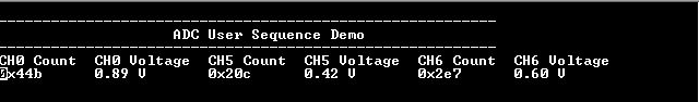
This example application shows how to sample three analog inputs using the user sequencer in software trigger mode and send the converted data to the console.
Description
Conversion of the three analog inputs is triggered from software trigger at every 500 ms. The user sequencer is used to define the order of conversion:
| Board | Sequence of conversion |
|---|---|
| SAMA5D2 Xplained Ultra Evaluation Kit | AD5 –> AD6 –> AD0 |
Analog input voltage in the range of 0 V to 3.3 V is fed to the ADC input channel AD5, AD6 and AD0. ADC conversion result is displayed on the console.
Downloading and building the application
To clone or download this application from Github, go to the main page of this repository and then click Clone button to clone this repository or download as zip file. This content can also be downloaded using content manager by following these instructions.
Path of the application within the repository is apps/adc/adc_user_sequence/firmware .
To build the application, refer to the following table and open the project using its IDE.
| Project Name | Description |
|---|---|
| sam_a5d2_xult.X | MPLABX project for SAMA5D2 Xplained Ultra Evaluation Kit |
Setting up AT91Bootstrap loader
To load the application binary onto the target device, we need to use at91bootstrap loader. Refer to the at91bootstrap loader documentation for details on how to configure, build and run bootstrap loader project and use it to bootstrap the application binaries.
Setting up the hardware
The following table shows the target hardware for the application projects.
| Project Name | Board |
|---|---|
| sam_a5d2_xult.X | SAMA5D2 Xplained Ultra Evaluation Kit |
Setting up SAMA5D2 Xplained Ultra Evaluation Kit
Setting up the board
- Short jumper JP2 (DEBUG_DIS)
- Connect the Debug USB port on the board to the computer using a micro USB cable
- Use a jumper wire to connect Pin 2 of J8 (AD0 is mapped to Port Pin PD19) to 3.3 V or GND
- Use a jumper wire to connect Pin 7 of J8 (AD5 is mapped to Port Pin PD24) to 3.3 V or GND
- Use a jumper wire to connect Pin 6 of J20 (AD6 is mapped to Port Pin PD25) to 3.3 V or GND
Running the Application
- Build the application using its IDE
- Open the Terminal application (Ex.:Tera term) on the computer.
- Connect to the EDBG/Jlink Virtual COM port and configure the serial settings as follows:
- Baud : 115200
- Data : 8 Bits
- Parity : None
- Stop : 1 Bit
- Flow Control : None
- The console displays the ADC Count and the ADC Input Voltage